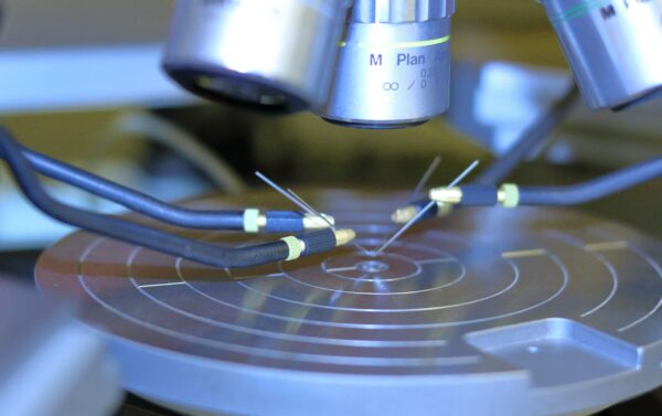
Microscopy
Microscopy Topics and Sections
From concept to commissioning, we guide you through every step:
1. Types of Microscopy
Microscopy is the technique used to magnify and visualize structures that are too small to be seen with the naked eye, typically utilizing lenses, beams of light, or electron waves. Optical microscopes use visible light and glass lenses to achieve magnification, while electron microscopes employ electron beams for much higher resolution imaging. There are also specialized types, such as fluorescence and confocal microscopy, which enhance contrast and provide three-dimensional imaging of biological or material samples.
The resolution of a microscope is determined by the wavelength of the illuminating source and the numerical aperture of the objective lens. Advances in microscopy, such as super-resolution techniques, have pushed the limits of resolution beyond traditional diffraction limits, enabling nanoscale imaging. Microscopes come in various types with each designed for specific applications and levels of magnification. There are four main types of microscopes.
A) Optical Microscopes (Light Microscopes)
Optical microscopes, also known as light microscopes, are instruments that use visible light and a system of lenses to magnify small objects for detailed examination. They typically consist of an objective lens, which collects light from the sample and magnifies the image, and an eyepiece lens, which further enlarges the image for observation.
The resolution of an optical microscope is limited by the diffraction of light, typically around 200 nanometers (according to Abbe’s diffraction limit). Different contrast-enhancing techniques, such as phase contrast, differential interference contrast (DIC), and fluorescence microscopy, improve visualization of transparent or weakly scattering samples.
Modern optical microscopes may incorporate digital imaging systems and computer-assisted analysis to enhance visualization and data collection.

B) Electron Microscopes
An electron microscope is a high-resolution imaging device that uses a focused beam of electrons instead of visible light to magnify structures at the nanometer or atomic scale. Due to the much shorter wavelength of electrons compared to light, electron microscopes achieve significantly higher resolution, allowing visualization of cellular structures, nanoparticles, and atomic arrangements. There are two main types: the scanning electron microscope (SEM), which provides detailed surface images, and the transmission electron microscope (TEM), which reveals internal structures by transmitting electrons through ultra-thin samples.
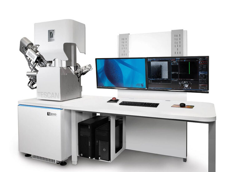
Author: Petrsk. Unedited Image.
C) Scanning Probe Microscopes (SPM)
A scanning probe microscope (SPM) is a high-resolution imaging tool that uses a physical probe to scan the surface of a sample at the nanometer or atomic scale. Unlike optical or electron microscopes, SPM relies on interactions between the probe and the sample, such as atomic forces or tunneling currents, to generate topographical and material property maps. Common types include atomic force microscopy (AFM) and scanning tunneling microscopy (STM), which provide detailed surface characterization with sub-nanometer precision.
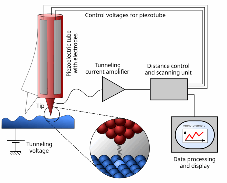
Author: Michael Schmid and Grzegorz Pietrzak. Unedited Image.
D) X-Ray Microscopes
An X-ray microscope is an imaging device that uses X-rays instead of visible light to achieve high-resolution magnification of structures at the nanoscale. By utilizing the shorter wavelength of X-rays, it can penetrate samples and generate detailed internal images with higher resolution than optical microscopes, without the need for sectioning. X-ray microscopy is commonly used in materials science, biology, and nanotechnology, with techniques such as soft X-ray microscopy and X-ray tomography enabling three-dimensional visualization of complex structures.
2. Optical (Light) Microscopes
Optical Microscopes use visible light and lenses to magnify small objects. There are several types of optical microscopes:
A) Brightfield Microscopes
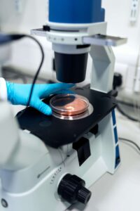
These are optical microscopes that use visible light to illuminate specimens, producing a bright background with darker samples. It consists of a light source, condenser lens, objective lenses, and an eyepiece or camera to magnify the image. A wide variety of accessories add varied functionality. Light passes through (or around) the specimen, and contrast is generated by the differential absorption or scattering of light by the sample.
Since unstained specimens may appear transparent, biological samples are often stained to enhance visibility. The resolution is typically limited by the wavelength of visible light, but high-quality objective lenses improve image clarity. Solid specimens will appear largely dark but with a well-defined edge.
Brightfield microscopy is widely used in biology, microbiology, and histology for examining cells, tissues, and microorganisms. It is also used in manufacturing where measuring microscopes are used for incoming part inspection, and end-of-the-line component quality control.
B) Darkfield Microscopes
These are optical microscopes that enhances contrast by illuminating the specimen with oblique light, preventing direct light from entering the objective lens. This creates a dark background, while light scattered by the specimen appears bright, making fine structures more visible.
A special darkfield condenser with a central stop blocks direct light and allows only refracted or diffracted light to reach the objective. This technique is useful for observing transparent, unstained, or live specimens that would be difficult to see under brightfield illumination. Special darkfield lights may also be utilized.
Darkfield microscopy is commonly used in microbiology to visualize bacteria, spirochetes, and other small structures with high contrast. This requires careful sample preparation, as thick specimens or highly refractive materials can cause image distortions.

Author: Zephyris. Unedited Image.
C) Phase-Contrast Microscopes
These are optical microscopes designed to enhance the contrast of transparent and unstained specimens by exploiting differences in their refractive indices. It uses a phase plate and an annular diaphragm to shift the phase of light waves passing through the specimen, converting phase differences into intensity variations. This process enhances the visibility of internal structures, such as organelles in live cells, without requiring staining.
The technique is particularly useful for observing living cells, microbial cultures, and thin tissue sections. Phase-contrast microscopy provides high-contrast images but can introduce halo artifacts around structures.
It is widely used in cell biology, microbiology, and medical diagnostics for non-invasive specimen examination.
D) Fluorescence Microscopes
These are optical microscopes that uses high-energy light, typically ultraviolet (UV) or blue light, to excite fluorescent molecules in a specimen, causing them to emit light at a longer wavelength. It employs special optical filters to selectively transmit the emitted fluorescence while blocking the excitation light, enhancing contrast and specificity.
Fluorophores, such as dyes or genetically encoded fluorescent proteins, bind to specific cellular structures, enabling highly detailed visualization of biological molecules and processes. The microscope typically includes a mercury, xenon, or LED light source, dichroic mirrors, and objective lenses optimized for fluorescence imaging.
Fluorescence microscopy is widely used in cell biology, immunology, and medical diagnostics for studying proteins, organelles, and dynamic cellular events. Advanced techniques such as confocal and super-resolution fluorescence microscopy further improve resolution and depth of imaging.
Author: Masur. Unedited Image.
E) Confocal Laser Scanning Microscopes (CLSMs)
These are advanced optical microscopes that use laser illumination and a pinhole aperture to achieve high-resolution, optically sectioned images of specimens. The laser scans the sample point by point, and only in-focus light is detected, while out-of-focus light is blocked by the pinhole, significantly improving contrast and depth resolution. Multiple images can be acquired at different focal planes to generate 3D reconstructions of complex structures.
Fluorescent dyes or proteins are often used to label specific cellular components, making CLSMs ideal for studying biological specimens with high specificity. The system typically includes photomultiplier tubes (PMTs) or other sensitive detectors to capture emitted fluorescence signals with high precision.
CLSMs are widely used in biomedical research, neuroscience, and materials science for imaging thick specimens, live cells, and subcellular structures with superior clarity.
3. Electron Microscopes
Electron microscopes use electron beams instead of light to achieve extremely high magnification and resolution. There are three common types of electron microscopes:
A) Transmission Electron Microscopes (TEMs)
These microscopes that use a beam of high-energy electrons to illuminate a thin sample, providing high-resolution images at the nanometer scale. Electrons pass through the specimen, and those that are transmitted are focused by magnetic lenses onto a detector, producing an image with much higher resolution than light microscopes. The sample must be extremely thin (typically less than 100 nanometers) to allow electron penetration.
TEMs are capable of resolving fine details of cellular structures, subcellular organelles, and even individual molecules. The high magnification and resolution of TEM make it invaluable in fields such as materials science, nanotechnology, and cell biology. Sample preparation is complex often requiring fixation, dehydration, and sectioning before imaging.

Author: Gringer. Unedited Image.
B) Scanning Electron Microscopes (SEMs)
These microscopes scan the surface of a specimen with a focused beam of electrons, generating high-resolution, 3D images of the surface topography. Unlike Transmission Electron Microscopes (TEMs), SEM s do not transmit electrons through the sample but detects secondary or backscattered electrons emitted from the surface. These electrons are collected by detectors and converted into an image that provides detailed information about the surface morphology, texture, and composition.
SEMs offer a high depth of field, allowing for the examination of large and uneven surfaces with great clarity. The specimens used in SEMs are typically coated with a thin layer of conductive material, like gold, to prevent charging.
SEMs are widely used in materials science, biology, and industrial applications for studying surface features at the micrometer to nanometer scale.
C) Cryo-Electron Microscopes (Cryo-EMs)
These microscopes are a specialized type of electron microscope that allows the imaging of biological samples in their native, hydrated state without the need for staining or fixation. The specimen is rapidly frozen to preserve its structure and then imaged at extremely low temperatures, typically under liquid nitrogen conditions, to prevent damage from radiation or dehydration. Cryo-EMs use transmission electron microscopy principles but requires specialized equipment to handle frozen samples and collect data at low temperatures. It is particularly powerful for imaging large biomolecular complexes, proteins, and viruses in three dimensions.
The technique can provide near-atomic resolution images, making it a revolutionary tool in structural biology, particularly for studying macromolecular structures that are difficult to crystallize. Cryo-EM has gained widespread use in drug design, molecular biology, and biomedical research.
4. Scanning Probe Microscopes (SPMs)
SPMs use physical probes to scan surfaces at the atomic or molecular level.
A) Atomic Force Microscopes (AFMs)
These microscopes that use an ultra-sharp tip mounted on a flexible cantilever to scan the surface of a specimen at the atomic or nanometer scale. As the tip interacts with the surface, it detects variations in surface topography, stiffness, and other mechanical properties through deflections in the cantilever. The deflections are measured using a laser beam reflected off the back of the cantilever into a photo-detector, allowing precise 3D imaging of the surface.
AFMs can operate in several modes, including contact mode, tapping mode, and non-contact mode, to measure surface roughness, elasticity, and other nanoscale characteristics. It provides high-resolution imaging without the need for a vacuum or sample preparation, making it versatile for biological, material science, and nanotechnology applications.
AFM are especially useful for imaging surfaces at the atomic scale, studying molecular interactions, and characterizing mechanical properties of materials.
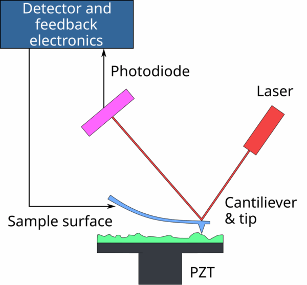
Author: OverlordQ
B) Scanning Tunneling Microscopes (STMs)
These microscopes are a type of scanning probe microscope that uses a sharp metal tip to scan the surface of a conductive material at an atomic scale. The microscope relies on the quantum tunneling effect, where electrons “tunnel” between the tip and the surface when they are extremely close (on the order of angstroms).
The tunneling current is measured and used to create high-resolution images of the surface’s atomic structure. STMs can also be used to manipulate individual atoms and molecules, enabling precise control at the nanometer scale. This technique requires the sample to be conductive and is typically used in surface science, nanotechnology, and materials research.
STMs provides detailed atomic-level imaging and is capable of resolving features at the single-atom level, making it a powerful tool for studying materials and molecular interactions.
5. X-Ray Microscopes
These microscopes use X-rays instead of visible light to image a specimen, allowing for high-resolution imaging of dense or thick samples that are opaque to visible light. X-ray microscopes typically operate using synchrotron radiation or specialized X-ray tubes as the light source, and employ focused X-ray beams to scan the sample. The X-rays interact with the sample, and the transmitted or fluorescent X-ray signals are detected by a detector to create an image.
This technique can provide detailed internal views of biological tissues, materials, and complex structures without the need for sectioning or staining. X-ray microscopy is particularly useful for studying the internal structure of materials, biological samples, and microstructures at the micrometer to nanometer scale. Due to the penetrating nature of X-rays, it allows for non-destructive imaging of thick or highly attenuating specimens.
6. Common Microscope Accessories
Microscopes can be equipped with a variety of accessories to enhance their functionality and improve imaging capabilities. Below are the most common accessories, their functionality, and the types of microscopes that typically use them.
Microscope Types that commonly use the noted accessory.
“Optical” = Optical Microscope
“Electron” = Electron Microscope
“SPM” = Scanning Probe Microscope
“X-Ray” – X-Ray Microscope
A) Illumination Accessories
- LED or Halogen Light Sources – Provide stable, intense and adjustable lighting. (Optical)

- Darkfield Lighting & Condensers – Enhance contrast for transparent specimens. (Optical)
- Phase Contrast Accessories – Improve visibility of transparent or unstained samples. (Optical)
- Polarizing Filters – Reduce glare and enhance contrast for birefringent materials. (Optical)
B) Lenses & Optics
- Objective Lenses – Different magnifications (4x, 10x, 40x, 100x) for varying detail levels. (Optical)
- Eyepieces (Ocular Lenses) – Typically 10x, but can vary. (Optical)
- Oil Immersion Lenses – Provide high-resolution imaging for 100x magnification. (Optical)
- Auxiliary Lenses – Used to expand the magnification range. (Optical)
C) Specimen Preparation & Handling Accessories
- Stage Micrometers – Used for calibration and measurements. (Optical)
- Mechanical Stages – Allow micron-resolution movement of the specimen. (Optical)
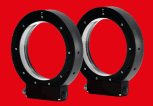
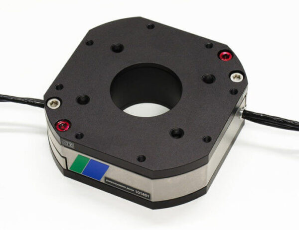
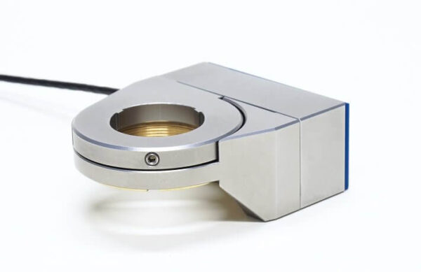
- Piezo Nanopositioning Stages – Allows for sub-nanometer resolution and precision movement of the specimen. (Optical, SPM)
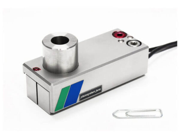
- Objective Positioners – Allows for sub-nanometer objective focusing. (Optical)
- Slide Holders & Clips – Keep the specimen slide in place. (Optical)
- Heating Stages – Maintain or control sample temperature. (Optical)
- Ultramicrotomes – For slicing ultrathin sections of specimens. (Electron)
- Sputter or Carbon Coaters – For applying a thin conductive metal layer to enhance contrast. (Electron)
- Cryo-Preparation & Ion Beam Milling Systems – For freezing and thinning samples. (Electron)
- Tilting & Rotating Holders – For multi-angle imaging. (Electron, X-Ray)
- Cryo & Heating Stages – Low & high temperature maintaining stages. (Electron, SPM, X-Ray)
- Environmental Chambers – For maintaining specific temperature, humidity or gas conditions. (Electron, SPM)
- Focused Ion-Beam Systems – To modify specimens at the nanoscale. (Electron)
- Micromanipulators – Enable precise sample positioning. (Electron, X-Ray)
- Sample Holders – Magnetic or vacuum-based. (SPM)
- Vacuum Chambers – For reduced air absorption. (X-Ray)
- Vibration Isolation Tables/Chambers – To minimize sample movement for precision viewing and imaging. (Optical, SPM)
D) Filtering Enhancements, Imaging & Recording Devices
- Neutral Density Filters – Reduce light intensity without altering color. (Optical)
- Color Filters – For enhancing contrast in certain applications. (Optical)
- Fluorescence Filters – To separate excitation and emission wavelengths. (Optical, X-Ray)
- Digital Cameras – Attach to the microscope for capturing images and videos. (Optical, X-Ray)
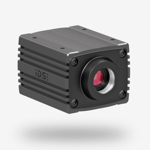
- USB or Wi-Fi Adapters – Enable connection to computers or mobile devices. (Optical)
- Image Processing Software – Enhance and analyze images, and to measure samples. (Optical, Electron, X-Ray)
- Tomographic Reconstruction Software – To convert 2D projections into 3D images. (X-Ray)
- Electron Detectors – For providing topographical and compositional contrast. (Electron )
- Energy Dispersive & Wavelength Dispersive Spectroscopy detectors – For identifying elemental composition. (Electron)
- Optical Detection Systems – Tip-sample interaction monitoring. (SPM)
- Raman Spectroscopy Integration – For adding Raman Spectroscopy for chemical analysis. (SPM)
- Kelvin Probe Force Microscopy Module – To measure surface potential variations. (SPM)
- Scanning Tunneling Spectroscopy Modules – To analyze electronic states at the atomic level. (SPM)
- Nanoindentation Accessories – For measuring mechanical properties at the nanoscale. (SPM)
- Absorption Contrast Filters – For enhancing contrast of specific materials. (X-Ray)
- Scintillator Screens – Converts X-rays into visible light for imaging. (X-Ray)
- Photon-Counting Detectors – Improves sensitivity and contrast. (X-Ray)
- Phase Contrast imaging Modules – Enhance visualization of weakly absorbing structures. (X-Ray)
E) Measurement & Analysis Tools
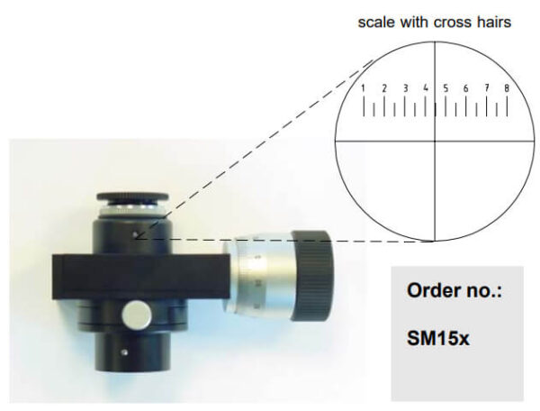
- Micrometer Reticles – Placed inside the eyepiece for measuring specimens. (Optical)
- Telecentric Objective Lenses – For precision measurement of a specimen. (Optical)
- Software for Image Analysis – Used for detailed sample examination, measurement to .5 microns & documentation. (Optical)
F) Vacuum and Maintenance Accessories
- Vacuum Pumps (rotary, Turbo, Ion) – Maintains vacuum levels. (Electron)
- Desiccators – For store moisture-sensitive samples. (Electron)
- Plasma Cleaners – Removes contaminants from samples and holders. (Electron)
G) X-Ray Sources & Optics
- Microfocus X-Ray Tubes – Provide high-resolution imaging with small focal spots. (X-Ray)
- Synchrotron Radiation Sources – Used for ultra-resolution and specialized research applications. (X-Ray)
- Zone Plates – Act as X-Ray lenses to focus and magnify images. (X-Ray)
- X-Ray Mirrors and Condensers – Improve beam focusing and illumination. (X-Ray)
H) Probe & Cantilever Accessories
- AFM Tips and Cantilevers – Typically made of silicon or silicon nitride, these tips have various shapes for different imaging modes. (SPM)
- Conductive AFM Tips – Used for electrical measurements. (SPM)
- Magnetic AFM Tips – used for Magnetic Force Microscopy. (SPM)
- High-Aspect-Ratio Tips – Allows for imaging of deep features in high-resolution applications. (SPM)
7. Common Microscopy Applications
Microscopes use their specialized functionality and unique imaging capabilities for a wide variety of research and industrial applications. Below are the most common applications and which microscope types are commonly used.
Microscope Types that are commonly used in the following applications.
“Optical” = Optical Microscope
“Electron” = Electron Microscope
“SPM” = Scanning Probe Microscope
“X-Ray” – X-Ray Microscope
A) Biomedical, Healthcare & Life Sciences
- Pathology & Histology – Disease diagnosis, cell and tissue imaging & analysis. (Optical, Electron, X-Ray)
- Microbiology – Bacteria, fungi, and viruses study and visualization. (Optical, Electron)
- Cellular Biology – Cell surface structure and function analysis. (Optical, Electron)
- Clinical & Diagnostic Labs. (Optical)
- Biomaterial Research – Artificial tissues & implants. (Electron)
- Neuroscience and Brain Tissue Examination. (Electron)
- Nanoscale Imaging – For biomolecules, proteins and DNA. (SPM)
- Drug delivery system characterization and imaging. (SPM, X-Ray))
- Mechanical properties of biological tissues. (SPM)
- 3D visualization of soft tissue structures without staining. (X-Ray)
- Examination of bone microarchitecture. (X-Ray)
B) Pharmaceuticals
- Drug formulation microstructure analysis and coating quality control. (Optical, SPM, X-Ray)
- Contamination detection. (Optical, Electron, X-Ray)
- Pharmacological research. (Optical)
- Nanoparticle drug formulation and delivery system analysis. (Electron, SPM)
- Quality control of drug formulations. (Electron)
- Protein structure and crystallography. (Electron)
- Surface adhesion and interaction studies. (SPM)
- Quality control of biomaterials. (SPM)
- Non-Destructive inspection of tablets and coatings. (X-Ray)
C) Electronics & Semiconductor Industry
- PCB inspection and quality control. (Optical, Electron)
- Semiconductor wafer analysis. (Optical)
- Nanoscale surface characterization of semiconductors. (SPM)
- Micro-soldering and component placement. (Optical)
- Failure analysis and defect detection in microchips and PCBs. (Electron, SPM, X-Ray)
- Wafer inspection. (Electron)
- Nanostructure and thin-film analysis. (Electron, SPM)
- Conductivity and electrical property mapping. (SPM)
- 3D imaging of wafers and microchips. (X-Ray)
- Solder joint defect detection. (X-Ray)
- Inspection of micro-electromechanical systems (MEMS). (X-Ray)
D) Material Science & Metallurgy
- Metallurgical analysis (grain structure, fractures). (Optical, Electron, SPM)
- Failure analysis in materials. (Optical, Electron)
- Surface defect inspection. (Optical)
- Composite material and polymer characterization. (Electron)
- Corrosion and surface treatment studies. (Electron)
- Atomic-scale imaging of metals/alloys. (SPM)
- Friction, wear, and hardness measurements at the nanoscale. (SPM)
- Internal structure and defect analysis in metals, composites, welded and bonded surfaces. (X-Ray).
- Microstructural studies of ceramics and polymers. (X-Ray)
- Non-destructive testing of advanced materials. (X-Ray)
E) Nanotechnology and Advanced Materials & Manufacturing
- Micro& nano-fabrication process monitoring. (Optical, Electron)
- Nanomaterial research and quality control. (Optical, Electron, SPM)
- 3D printed material analysis. (Optical)
- Carbon nanotube and graphene analysis. (Electron, SPM)
- Surface coating and then-film inspections. (Electron)
- 3D surface topography of nanostructures. (SPM)
- Mechanical, electrical, and magnetic property mapping. (SPM)
- Nanomechanical testing for material durability. (SPM)
- Medical device and implant quality control. (X-Ray)

F) Forensics & Criminal Investigation
- Trace evidence analysis – hair, fibers, gunpowder residue. (Optical, Electron, X-Ray)
- Document verification – ink and paper analysis. (Optical, Electron)
- Counterfeit detection and analysis in documents and currency. (Optical, Electron, SPM, X-Ray)
- Toolmark and ballistic investigations. (Electron)
- Nanostructure analysis. (SPM)
- Coatings & security materials analysis. (SPM)
- Examination of hidden features in forensic evidence. (X-Ray)
- Investigation of explosives and concealed materials. (X-Ray)
G) Aerospace & Automotive Industry
- Failure analysis of aerospace materials and components. (Electron, X-Ray)
- Composite material integrity testing. (Electron)
- Wear analysis of automotive parts. (Electron)
- Inspection of coatings and protective layers. (Electron)
- Surface analysis of lightweight composites. (SPM)
- Nanoscale wear analysis of turbine blades and engine components. (SPM)
- Corrosion and fatigue studies in aerospace alloys. (SPM)
- Lubrication and adhesion studies of automotive materials. (SPM)
- Non-destructive testing of composite materials. (X-Ray)
- Internal defect detection in engine and structural components. (X-Ray)
- Additive manufacturing (3D printed parts) quality control. (X-Ray)
H) Environmental Science, Energy & Agriculture
- Soil and water contamination analysis. (Optical)
- Insect and plant pathology studies. (Optical)
- Microplastic and nanoparticle pollutant analysis in air, water & soil. (Optical, Electron, SMP)
- Mineralogy and geoscience applications. (Electron)
- Battery and fuel cell material development. (Electron)
- Solar cell microstructure imaging and efficiency optimization. (X-Ray, SPM)
- Nanoscale corrosion and wear analysis in energy materials. (SPM)
- Water filtration membrane analysis. (SPM)
- Battery failure analysis. (X-Ray)
- Fuel cell material characterization. (X-Ray)
- 3D imaging of rock and mineral structures. (X-Ray)
- Microfossil and paleontology studies. (X-Ray)
I) Education & Research
- University and institutional research in physics, chemistry and (Optical, Electron, SPM)
- STEM education for nanoscience and surface analysis learning. (Optical, Electron, SPM)
- Advancing research in diverse scientific fields such as nanotechnology. (Optical, Electron, SPM)
8. Microscopy Technical Terms
Resolution – The ability of a microscope to distinguish two points as separate; typically measured as the smallest distance between two objects that can be clearly distinguished.
Magnification – The process of enlarging the appearance of an object, usually by a microscope or optical system.
Objective Lens – The lens closest to the specimen, responsible for primary magnification and resolving power in microscopes.
Eyepiece (Ocular Lens) – The lens through which an observer looks, usually providing additional magnification.
Field of View – The observable area seen through the microscope, typically measured in millimeters or micrometers.
Depth of Field – The range of focus in a sample that appears sharp and in focus at any given moment.
Contrast – The difference in light intensity between the image and its background, enhancing the visibility of different parts of the specimen.
Phase Contrast – A microscopy technique that enhances the contrast in transparent specimens by converting phase shifts into visible changes in intensity.
Fluorescence – Emission of light by a substance that has absorbed light or other electromagnetic radiation, often used in fluorescence microscopy to visualize specific structures.
Chromatic Aberration – A distortion caused by the inability of a lens to bring all wavelengths of light to the same focal plane.
Working Distance – The distance between the front of the objective lens and the specimen when the sample is in focus.
Numerical Aperture (NA) – A dimensionless number that characterizes the range of angles over which the lens can accept or emit light, directly affecting resolution.
Electron Microscope – A type of microscope that uses a beam of electrons to create an image, achieving much higher magnifications than light microscopes.
Scanning Electron Microscope (SEM) – A type of electron microscope that scans the surface of a specimen with a focused beam of electrons to generate detailed 3D images.
Transmission Electron Microscope (TEM) – A microscope that transmits electrons through a thin specimen, producing high-resolution 2D images of internal structures.
Confocal Microscopy – A technique that uses a laser to scan a specimen and create high-resolution, optically sectioned images, often used for 3D reconstructions.
X-Ray Microscope – A type of microscopy that uses X-rays instead of visible light to produce images of dense or thick specimens.
Cryo-EM (Cryo-Electron Microscopy) – A method in electron microscopy that involves freezing samples and imaging them at cryogenic temperatures to preserve their natural state.
Atomic Force Microscope (AFM) – A type of scanning probe microscope that measures surface roughness and mechanical properties by scanning with a sharp tip.
Scanning Tunneling Microscope (STM) – A microscope that uses quantum tunneling to image surfaces at the atomic scale by scanning a sharp metal tip across a conductive surface.
Super-Resolution Microscopy – A class of microscopy techniques that break the diffraction limit of light to achieve resolution beyond the typical limits of optical microscopy.
Focal Plane – The plane of a specimen that is in focus, corresponding to the level at which light converges to produce a sharp image.
Dichroic Mirror – A mirror used in fluorescence microscopy that reflects light of a specific wavelength while allowing other wavelengths to pass through.
Monochromatic Light – Light consisting of a single wavelength, often used in specific types of microscopy for precise illumination.
Staining – The process of applying colored dyes to specimens to enhance contrast and make specific structures more visible under a microscope.
Refractometer – An instrument used to measure the refractive index of materials, important in optical microscopy to understand light interactions with the sample.
Light Source – The illumination used in light microscopes, often a halogen lamp, LED, or mercury vapor lamp.
Optical Sectioning – A technique used in microscopy to capture thin slices or planes of a specimen, allowing for 3D imaging by compiling multiple sections.
Birefringence – The property of a material to split light into two beams, used in polarized light microscopy to study internal stress or structures in samples.
SNR (Signal-to-Noise Ratio) – A measure of the clarity of an image, representing the ratio of useful signal to background noise, with a higher SNR leading to better image quality.
Want to learn more?
Address
1 Cabot Road, Suite 210 Hudson, MA 01749
Call Us
1-508-634-6688